jMIPS |
an open source MIPS processor in Java |
| Prev | Next |
A MIPS processor in JavaThis is the jMIPS easy-to-use open-source MIPS processor in Java. You should already have downloaded the archive (up to date copies are on the jMIPS project pages) within which this documentation is to be found as the contents of the doc/html subdirectory.
Getting to know the software here greatly aids learning about the MIPS hardware architecture and also creates familiarity with more general concepts of computer systems and architectures. There are five processor models to look at and play with in the archive, identified here as 1 to 5. The numbers increase with increasing sophistication in the model, thus:
The following pages will take you through the process of using and perhaps building the basic processor model in detail, and then go on to consider the other models. The models do not differ in how they are built or used - it's only the innards that are different in each case and that results in one model being faster than another in the same context. You will want to get to work with each model processor in turn, perhaps with the aim in mind of improving the model to get it to run faster still. How long it takes to run overall and per instruction is one of the default printed outputs. If you want to get out statistics such as how long each class of instruction takes to execute in particular circumstances, you will have to add in the code for that yourself. It's open source! You can do that. The code is clearly written and explained in the pages here.
How to run the basic MIPS processor modelThere should be a Java archive file (a jar) in the supplied zip archive or compressed tar file (get one of them from the download link on the project page). If there isn't, then go to the next section. You should extract the jar file from the archive with (for example, the archive name depending on your download choice) % unzip jMIPS-1.7.zip jMIPS-1.7/lib/CPU.jar or % tar xzvf jMIPS-1.7.tgz jMIPS-1.7/lib/CPU.jar Also extract some of the contents of the misc directory with % unzip jMIPS-1.7.zip jMIPS-1.7/misc/hello_mips32 or % tar xzvf jMIPS-1.7.tgz jMIPS-1.7/lib/hello_mips32 then the Cpu1 class can be run by a Java Virtual Machine (JVM) on any platform. You might do so under Linux with % java -cp jMIPS-1.7/lib/CPU.jar CPU.Cpu1 -q jMIPS-1.7/misc/hello_mips32 For example: % java -cp jMIPS-1.7/lib/CPU.jar CPU.Cpu1 -q jMIPS-1.7/misc/hello_mips32 Hello world % If you are unpacking the 1.7d or later archive, you'll get a GUI to launch the five pre-built models with. Run % jMIPS-1.7d/lib/CPU.jar % 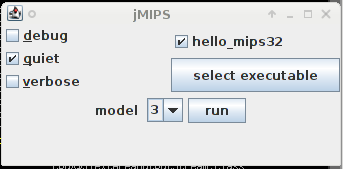 and you'll get the window shown at right. It's already been used to pick out a hello_mips32 executable file from the misc/ subdirectory of the source archive, so that's shown as available and by default ready to run; and the "quiet" switch has already been selected too! To change the CPU model (set at "3" in the image), use the "model" control. Then hit "run" and a window will pop up containing the output from the run. How to compile the basic MIPS processor modelIf you want to or have to compile the Java source code to get executable code, you would do so as follows, depending on which tools you have available. Since there are different sets of tools that people are used to using on different operating systems, the following subsections are specific to an operating system. Compiling under Linux or UnixIf you are on a Mac, and use a HFS or HFS+ format file system, go into the system properties and turn on case sensitivity for it. You will need that as otherwise you will get case folding bringing several file names into collision with each other, which you do not want. Unarchive the zip or compressed tar file (get them from the project page download link) with % unzip jMIPS-1.7.zip or % tar xzvf jMIPS-1.7.tgz respectively. Then find the src/ directory in the newly unpacked file hierarchy and change your current directory to it (use the cd jMIPS-1.7/src change directory command to do so). I prefer to produce generic Java bytecode for a Java Virtual machine (JVM), with % javac CPU/Cpu1.java in the src/ directory, and then the resulting Cpu1.class file can be run by a JVM on any platform. You might do so under Linux with % java CPU/Cpu1 -q ../misc/hello_mips32 For example: % java CPU/Cpu1 -q ../misc/hello_mips32 Hello world % Building a jar file is just a question of first building all the java class files:
% javac CPU/*.java
%
and then making a jar file with % jar cf ../lib/CPU.jar CPU/*.class % In reality, a jar is just a zip archive of the package done without compression, and with one extra manifest file also included. So you can make it using just a zip archiver and you don't necessarily need the jar tool. Look up the details on Java tutorials site or examine an existing jar file using the zip archiver for comparison. Compiling under WindowsTo import the source into a Java NetBeans IDE, start yourself a new NB project (called `jMIPS', presumably), making sure the IDE dialog's tick-boxes for `Main Class', etc, are all unchecked. Once the IDE has built all the directories and control files that it needs, copy the src/CPU/ directory *.java files from the source code archive to a new src/CPU/ subdirectory of the jMIPS project directory that has just been created by NetBeans. Use an operating system copy command straight from inside the zip archive, if possible, to avoid the files touching disk on the way. Windows may fold some of the file names otherwise. If Netbeans has a menu choice to import from zip, or compile from zip, that would be perfect. The IDE will detect you populating the source code area and it will expand its `Source Packages' tree view (the jMIPS/src directory) to include a CPU "package" and its Java files. If you'd rather, you can systematically rename the java class files for each processor model from Cpu1.java, Cpu2.java, etc, to, for example, WinCpu1.java, WinCpu2.java, etc. You will have to rename the class declared within each file to match. Notes on running a processor modelThe meaning of the command line options is as follows:
% java CPU.Cpu1  hello_mips32
0:      0.000000007s:   0x80030080:     addiu $29, $29, -32
1:      0.000000012s:   0x80030084:     sw $31, 28($29)
2:      0.000000019s:   0x80030088:     sw $30, 24($29)
3:      0.000000024s:   0x8003008c:     addu $30, $29, $0
4:      0.000000030s:   0x80030090:     sw $28, 16($29)
...
218:    0.000001567s:   0x8003000c:     lui $3, -20480
219:    0.000001573s:   0x80030010:     ori $3, $3, 16
220:    0.000001580s:   0x80030014:     sb $3, 0($3)
%
This run executed 220 instructions in 0.000001580 simulated seconds (the clock rate is 1 simulated GHz). That was around 5 clock ticks per instruction execution.
% java CPU.Cpu1 -q hello_mips32
Hello world
%
% java CPU.Cpu1 -d hello_mips32
text start at virtual addr 0x80030000 file offset 0x10000
text end   at virtual addr 0x800300e0 file offset 0x100e0
text entry at virtual addr 0x80030080 file offset 0x10080
read 224B at offset 65536 from file 'hello_mips32'
stack start at virtual addr 0xb0000000
stack end   at virtual addr 0xb0100000
0:      0.000000007s:   0x80030080:     addiu $29, $29, -32
1:      0.000000012s:   0x80030084:     sw $31, 28($29)
2:      0.000000019s:   0x80030088:     sw $30, 24($29)
...
%
Please do just edit away at the source in order to add anything else you like, add yourself to the credits list at the top of the source code in the file, and send in your changed code - or publish it yourself elsewhere, as you wish. Producing MIPS machine code to run in the processorThe "Hello world" program ready-built in MIPS R3000 machine code is in the archive as the hello_mips32 file in the misc/ subdirectory. The (C language) source code for it is in the hello_mips32.c file in the archive misc/ directory, and the MIPS assembler for it is the hello_mips32.s. The machine code has been compiled quite standardly from the given source to give the machine code, via % gcc -static -o hello_mips32 -Wl,-e,f hello_mips32.c on a real MIPS machine. Check the manual page for the gcc command (i.e., "man gcc") to find out exactly what the options given in this command line mean. On non-MIPS but Unix platforms, the following should achieve the same result using the mips-gcc cross-compiler suite (you may typically have to run a "setup MIPS" command in your shell environment in order to set your executable search path to pick up the cross-compiler's component parts):
% mips-gcc -DMIPS -mips1 -mabi=32 -c hello_mips32.c
% mips-ld -Ttext 0x80003000 -e f -o hello_mips32 hello_mips32.o
The software model of a MIPS processor stands in handily for a real MIPS machine when running the "Hello world" machine code. % java CPU/Cpu1 -q hello_mips32 Hello world However, more complicated machine code involving interrupts and peripherals might defeat this model.
Getting into the source codeHere are suggestions for how to get yourself "into" the source code, and having fun.
Edit it, credit yourself at top, and send the changes to the project. This is generally a good way to go about getting to know code. Complain about how badly written and difficult to understand it is, and fix it. You'll find copious notes on the code in the following section. You will want to look at the code with those notes in hand. The notes will prove most helpful in terms of understanding the large-scale features, leaving only nuances to be explained via source code comments.
First check on the web to see what the instructions do and what the machine code format for them is! One can say they must be a cross between a branch instruction and a jump-and-link instruction just from the name. Suppose bgezal is much the same as bgez but in the event of a successful test it does the same as a jal instruction does (places the address of the following instruction in the return address register, ra). That is useful for implementing a conditional subroutine call. Check google!
Test your modified emulator on the modified machine code. You'll need to make a compensating change to the program in order to save and restore the $ra return address register around the branch, but you'll see the new branch instruction itself working. Notes on the basic MIPS processor model codeThe regularity of the MIPS instruction set architecture results in very transparent simulator code. The simulator code has also been written with the objective of producing code that is clear without being over-sophisticated. 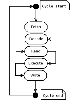 As a result, you can check out what any MIPS instruction does by eyeballing the appropriate area of the code. The CPU1 class code is imperative with just the minimum of object-oriented wrapping in order to make it easy to walk through. It's a state machine! And so it is, in reality. Whatever you need to see in order to understand the CPU1 processor model is in that code in the CPU1 class, and you need look nowhere else. You'll see there's just one big while loop in the code. It runs the generic Von Neumann fetch-decode-(read data)-execute-(write data) cycle (see accompanying figure at right), as implemented in all mainstream processor designs since the 1940s, and all the action is embedded inside this one long loop, with one short contiguous part dedicated to each kind of MIPS instruction. So you'll find there are about 10 or 12 shorter contiguous sections making up the body of the loop. For example, the part dealing with jump instructions looks like this ('fetch' has already been done at the start of the loop body, in order to read the next instruction into the IR register). It's mostly block comment:
That's just 6 lines of real code, not counting
the comment lines. In summary, the model encoded by the CPU1 class embodies an abstract Von Neumann processor design without low-level details of precisely how the electrons are being shuffled around and you should have no problem at all in looking at the code and understanding what it does as hardware (tip: when you look at a small section of any source code, look at it with a particular question in mind, such as figuring out how function X is used so you can make use of it yourself, and ignore everything else; repeat until done). The difference with respect to real hardware is that this code can only do one thing at a time, whereas real physics results in hardware doing all these things done in sequence here all at the same time during a processor cycle. However, execution is timed using the Clock class methods and the final accounting to you of what has happened only occurs when a complete processor cycle is up. So the order things are done in in software between those points does not particularly matter. So long as the order makes logical sense, the model works. For example, the jump code above writes the RA register with data read from the instruction in the IR register. In real hardware, those two things happen simultaneously, as the result of an electric potential field transmitted across a conductive wire. In the code above the read happens before the write, because the Java implementation requires it that way! We can't write in Java "read A and write the result into B simultaneously". The physics of the real universe makes that easy in reality! The accounting by the components involved, however, will record the same simulation time moment of occurrence for both the read and the write, and that is all you will see in the end. Class layoutThere are the following top-level classes in the source code, all in all. Only the first five or so contain any code worth discussing, and the discussion follows below the table:
This is a so-called domain-model design. The classes in the software code correspond to real physical components in the hardware MIPS processor. The methods correspond to actual physical operations that the hardware components can do. Virtual operations, such as those that can be composed as combinations of simpler operations, are never implemented in the software no matter how "convenient" it might seem, as they have no physical existence. 
The class diagram at right shows the dependencies. If you want to add a single-step facility to the Cpu1 simulator, you need to take the single big fetch-decode-execute while loop in the CPU1 code and make it pause for user input before each new cycle. You should make an s ("step") from the user execute another cyle; a c ("continue") should send it back to cycling continuously; a p ("print") and a register number or memory address should show the register or memory contents; a d ("display") should be like print but cause the printout to occur at every step. The main routine in Cpu1This is a quick and dirty precis of the main routine in Cpu1, the wrapper class whose job is to understand the Java command line arguments you used, and then set the CPU1 processor model going:
You see here that main parses the command line using the Cmdline analyse method, obtaining a list of executable files whose code it will run. The executable files are in what is known as `ELF format'. ELF is a cross-platform standard used in many operating systems in use today and it is the format produced by the gcc MIPS compilers and assemblers. The main routine then goes ahead and loads those ELF files. That is, it calls the Elf constructor on each file name, which parses the contents of the file and extracts information such as entry points, intended virtual address locations, etc., all of which get placed in the resulting Elf object. Then main builds the stack region of memory and the CPU, and tells the CPU's memory unit about the stack and its intended virtual address via a call to the memory unit's addRegion method. And it tells the memory unit about the various stretches of program code it has picked up from the ELF executable files via more calls to addRegion. It remains to set the CPU's SP (`stack pointer') register to point to the top of stack, set the CPU's PC (`program counter') register to the address of the intended program entry point - obtained from the first file named on the command line - and then call the newly built and prepped CPU's run method. That's all. So the following is all the programmer needs to know about Cpu1:
The next section shows you what the 'runs it' means. The CPU1 processor modelThe following is all the programmer can see or needs to know about the CPU1 processor class. There's a (pretty skeletel) constructor, and one method.
The run method code is not conceptually difficult. It's just the one big loop:
As it says in the comment, the loop contains the interior of the fetch-decode-execute cycle. Here it comes:
The abstract fetch/decode/(read)/execute/(write) sequence is clearly visible in the code. There's one conditional block dedicated to each kind of instruction (i.e., one per distinct opcode). The fragment above shows the block dedicated to treating ALU operations, which all have the opcode 0. The different kinds of ALU operation are distinguished by different values of the func field in the instruction (the last 6 bits at the least significant end of the word in bigendian layout). All the distinct fields of the instruction in the IR are broken out, including func, in the section labelled DECODE!, and then the instruction's functionality is implemented in the short Java code sections labelled READ!, EXECUTE!, WRITE! What's acceptable and what's not acceptable code in a processor modelNote that the code in the CPU1 run code is conscientiously using the emulated CPU hardware to do all the work. Instead of adding 4 to the PC value using the power of the Java programming language ("pc += 4"), for example, the FETCH section reads the PC using the PC register object's read method, adds 4 using the dedicated fetch adder's execute method, and routes the result back to the PC using the PC register object's write method. That's a long way round where "pc += 4" might have done the job! What's going on! What's allowed here and what's not? It is acceptable in the Java model to label values output by a hardware unit and use them as inputs to other hardware units. We've done that with 'pc = ...' and '... = pc'. That sort of thing amounts to using simple wiring to connect the data signals through the CPU circuitry within a single clock cycle. That's alright. But anything even as substantial as a +4 on the 'pc' would be cheating to do in Java because it takes time and circuitry to do it in real life. The Java objects standing in for the CPU hardware components (alu, register_unit, etc) have timing embedded in them and using them in the Java code makes the simulated clock advance correctly. They're OK to use for computations. Computations take time to do in real life. The Java objects methods advance simulated time. All OK. Using Java code like "pc+=4" would magically achieve the required effect without taking any simulated time and not occupy any of the simulated hardware in doing it either! That's not emulating the real life situation, that's emulating magic. Not OK. So any arithmetic has to be done using the Java objects representing CPU hardware components, not Java arithmetic. Because the DECODE section is done explicitly in inline Java code here, which makes it seem like it takes no time at all to do in simulated time, an explicit clock update has been embedded at the end of the DECODE code in order to keep the simulator timing honest. Contrariwise, the FETCH section needs no extra time update because the time taken is dominated by the instruction read from cache/memory, and the clock is updated properly via the memory unit access method call in that code section. The rule in writing simulator code like this is that one can use Java code variables to hold values but for no more than (less than) what is conceptually one simulated clock interval. They're like transitory signal values. Any signal value that is to persist for one simulated clock interval or more must be held in registers. That's what's done in the CPU1 run code. The notionally transitory pc and ir values are routed to the PC and IR for safekeeping across multiple clock intervals. The conf object that groups together the decode outputs looks like it persists, but as soon as the IR changes next cycle, the conf will be changed too. So it's conceptually just representing a set of wires hooked up to the IR via some decode circuitry and there is no extra storage involved. The CPU component classesThe remainder of this section documents the Java classes that represent components within the CPU. It's a reference document! You read a section just as and when you need to, and not before.
The RegisterUnit component classThis component comprises the 'small and super fast memory' inside the CPU.
RegisterUnit objects are composed of an array r of 32 (actually a little more in order to incorporate PC and IR as well) Register objects. There is nothing surprising in the read and write method codes. Read and/or write is all that can be done by or to hardware registers. The number of arguments says how many registers are being read and written at the same time (up to two reads and one write are supported, simultaneously). The 'byte' type for the register indices as arguments is just so you don't confuse the arguments that are the 5-bit indices of registers with the arguments that are the 32-bit contents of registers. Yes, we could use 'int' to represent both, but then you couldn't see which was which looking at the method type signature, and programming errors would follow on.
The only thing of any note is the automatic update of the clock when using the register unit. That guarantees that using this component leads to honest time accounting in the simulation. Reads and writes happen simultaneously. When we look at the Register component class code, we'll see that writes take effect next cycle, so one can do many distinct reads and one write to a register each cycle in the software, and it'll look as though it all happened at once in the simulator at the end of the cycle. The ALU classThe ALU component does the arithmetic within the CPU.
The ALU class is a substantial piece of code, but it's entirely simplistic. The execute method code consists of a large switch statement which chooses a short block of code to execute depending on the func (function code) value supplied as argument. The code combines the two input integers a and b in the appropriate way to produce the result c and a carry or zero indicator z:
The above illustrates only the addition operation code, but it is perfectly representative. None of the ALU code is any more complicated than that. The Memory component classThe Memory component represents random access memory (RAM) as seen by the CPU. The implementation here really mashes together two real hardware components, the memory manager and the memory units. It would be a bit of fussiness to separate out the two as two different components here, because we're not concerned with modeling memory in the same detail as we are modeling the CPU, and we would rather look at memory for the moment as a shiny, smooth, black box.
A memory object internally consists of an array of regions. These really exist as 'zone boundaries' configured into the memory manager side of our memory unit. Each region consists of a first address in memory, a last address, and a sequence of bytes representing the memory region content. In real life, once configured (and the configuration changes on the fly as one process after another enters the CPU), the memory manager imposes different policies on the different regions. One region may be read-only, another may be read-write. One may be cached, another not. The addRegion method is used to configure one more region into the memory unit. The read32be method then simply cycles through the array of regions looking for one which contains the supplied address for lookup, and returns the data stored in the region at the supplied offset when it finds the right region. The write32be method is complementary:
One might eventually want to signal an exception when a missing (i.e., unconfigured) region is addressed, but right now this code does the simple thing and ignores the problem. The memory unit also contains special read8 and write8 methods which read and write only one byte at a time. While they might seem like a convenience only (and indeed, internally they read and write 4 bytes at a time when they can using the read32be and write32be stalwarts), their real use is in performing memory mapped I/O. When the address supplied is right, the memory unit read8 and write8 methods pass the access attempt on to an iobus instead of to memory. Behind the bus and attached to it lie several I/O units. The code will be described in more detail below, but the most relevant thing to take in right now is that this arrangement means that talking to a special memory address allows characters to be read from the keyboard and printed to the screen. It's called memory-mapped I/O. The way the iobus intercepts are implemented inside the memory unit code is like this:
"0" is the I/O bus address of the console keyboard input, and "1" is the I/O bus address of the console display output. Via these intercepts, the memory unit translates reads from memory address GETCHAR_ADDRESS to reads from I/O bus address 0 which the bus translates to reads from the console attached to it. Similarly for PUTCHAR_ADDRESS and writes to the console. The memory unit's read8 code is more accurately represented as follows, with a loop over a port list instead of the hard-coded if statement address matches shown in the text above:
We could get away with adding a single port at a single memory address for the console unit, but I've preferred to cater for the general case in which PUTCHAR_ADDRESS and GETCHAR_ADDRESS are not necessarily the same, thus registering two different port addresses which give access to exactly the same console in exactly the same way. It's not a significant waste. It often happens in real life that I/O units have several alternative address mappings, all of which can be used for access. The redundancy is sometimes useful, and is often mandated for reasons of backwards-compatibility. The port list is appended to within the memory unit like this: port.add(new Port(GETCHAR_ADDR, 0)); // translation GETCHAR_ADDR -> bus 0 added port.add(new Port(PUTCHAR_ADDR, 1)); // translation PUTCHAR_ADDR -> bus 1 added In a later iteration of this code, you may wish to allow certain ports to be designated READ_ONLY or WRITE_ONLY! For now, each port is expected to support both reads and writes. Timing: raw access to memory is set to take MEMORY_LATENCY picoseconds, by default 2500, i.e., 2.5ns. You can change this value by fiddling with the MEMORY_LATENCY static variable in the Globals class. Or you can use "-o MEMORY_LATENCY=..." on the command line. Access to the I/O devices through the I/O bus address mappings takes a shorter time, nominally CACHE_LATENCY, which is set by default to 1000 picoseconds, i.e. 1ns. The idea is that on write all that happens is that the data is launched onto the I/O bus and then the CPU continues with its cycle. The I/O bus works on its own to send the data on to the printer (say), and the printer works on its own to buffer the data, and later print it out. On read all that happens is that the keyboard (say) device buffer is read via the bus for any characters previously typed. The ink is not sprayed on the paper, nor the keypress executed within the 1ns period itself. But how does the CPU cope with delays of the magnitude of memory acceses? They are longer than the nominal 1ns associated with the default clock rate of 1GHz and at least on read the memory access must take place fully within the CPU clock cycle. The answer is that the CPU executes a single exceptionally elongated cycle for a main memory read or write. The elongated cycle is of fixed duration but of such a length that the memory is able to respond within it. It's 2.5ns long, corresponding roughly to memory that can deliver 400MB/s. That's less than half as fast as L1 cache (which you'll meet in the CPU4 design). You will have to wait until you meet the CPU5 code to be able to improve on this design.
The IOBus component classThe IOBus is part of a three-way communication between CPU, memory, and it. When the CPU addresses certain places in memory, the access is redirected my the memory manager part of the memory unit to the IOBus instead. The IOBus class read8 and write8 methods take a bus address ("0", "1", etc.) instead of a memory address. The redirect substitutes a bus address for a memory address. There's an addIO method which registers an I/O unit (e.g. a Console object) onto the bus, which gives it a bus address. The bus addresses are awarded in order of registration to each I/O unit that wants one, in turn. As the CPU and memory unit is being put together, the bus is built and a single console is registered to the bus at both of bus addresses 0 and 1 like this: IOBus iobus = new IOBus(); Console console = new Console(); short stdin = iobus.addIO(console); // console registered as bus addr 0 short stdout = iobus.addIO(console); // console registered as bus addr 1 also Bus address 0 will be the mapping used for GETCHAR_ADDRESS within the memory unit, corresponding to reads from the console, and bus address 1 will be the mapping for PUTCHAR_ADDRESS, corresponding to writes to the console. The full interface to the I/O bus methods is
IOUnit is an abstract class ("interface"). Console objects match that interface. To meet the requirements of the interface an object just needs to have read8 and write8 methods. These methods don't take an address at all as they are conceptually associated with just their own I/O unit:
An IOUnit produces a byte on a read request, and absorbs a byte on a write request. Console objects in particular have these methods. The memory unit build code adds a console to the iobus and maps its bus address to a memory address via the port list. The upshot is that the console object is accessible over the iobus via memory mapped addressing from the memory unit. Why have we gone to the trouble of introducing a bus to mediate between the memory unit and what is at the moment a single I/O unit, a single console? It's really so that we can model delays introduced by the fact that the bus can only be used to access one I/O unit at a time, and only one byte at a time can travel down it (in one direction at a time), and the fact that the I/O bus in real life is relatively slow too - 33MHz, as compared to the CPU's 1GHz. The CPU can execute 30 instructions in the time that it takes 1 byte to travel down this I/O bus. If the memory unit tries to access the bus while it is already in use, there's trouble. Make sure that writes to the I/O bus are at least 30ns apart or you will find that trouble and strange things will start to happen like writes to the bus being discarded. In practice, it's not a deal-breaker. Whatever machine code you write, it's almost unheard of to produce a loop tight enough to do two writes to the I/O bus within 30ns. The CPU1 design struggles to deliver 6 machine instruction executions in that time. That's not enough to save registers, run a jump to a subroutine, do something, jump back, restore registers, increment a loop counter, check a loop bound, etc. There's code in there that makes a noise on the simulation error stream if the I/O bus ever gets swamped and it does not happen in practice. It could, though. For fun, try making it happen, by writing the appropriate machine code (via MIPS assembler, of course). You'll get a stream of imprecatory complaints on the screen. Real CPUs have their limits too, and real programmers write to them. You can write nearly anything you want in assembler, and whether the metal underneath can respond as you intend or not is a subtly different question. Real programmers follow the maxim of don't do that then. For example, if you check real MIPS assembler code you'll find that every jump instruction is followed by a NOP because nearly every real MIPS machine's pipeline and instruction prefetch mechanism makes it inevitable that the instruction after a jump will be executed! Miserly programmers could in theory save program text space by directly following a jump with a labelled non-trivial instruction, but they don't, because they know what will happen. Evolution has taught real programmers (the ones that survive to get their next paycheck and eat their next lunch) that reality is stronger than theory. Compilers don't do that then either, for the same reason. The StopClock component classOne more special I/O address mapping intercept is pre-set. It causes the Clock.stop method to be called when HALT_ADDRESS is written to, which ends the simulation!
There's really a special extra I/O unit called stopClock placed on the I/O bus to implement this. If you check out what the Memory code really looks like in the source file, you'll see instead of the above something like the following in the memory unit setup code: StopClock stopClock = new StopClock(); short stpclk = iobus.addIO(stopClock); // stopClock registered as bus addr 3 port.add(new Port(HALT_ADDRESS, stpclk)); // translation HALT_ADDR -> bus 3 added And the StopClock write8 method is only a thin wrapper round that vital call to Clock.stop.
If you are going to build more I/O units to implement special effects (perhaps audio?), the stopClock example provides you with the model for the way to go about it: first code the unit as a class with methods write8 and read8 that really do whatever you want, then make a new instance of the class at CPU or memory build time in the CPU code and put in a registration call with iobus.addIO for it, finally add a memory mapping intercept into the memory unit code. For best results do that last by updating the port list in the memory unit using port.add.
The Register component classRegisters are the components within the CPU that remember. Everything else starts each processor cycle as though it were starting anew each time. A register remembers what value it had last cycle. 32 addressable registers (and a few more) make up the register unit component in the CPU.
Register objects protect a single internal integer value. In principle, read and write methods simply access the integer, like this:
However, there's a twist. To better mimic the action of a real, clocked, register, we've arranged that the result of a write cannot be seen until the next clock tick. That is, reading the register shows the value stored in the register as of the last clock tick. You can write the register and read the register as you like during the period of a single clock tick, but reading will always show the same old value. After you call Clock.sync then reads will start showing the value that you wrote last before the Clock.sync call. To implement that we've added a variable xtick that holds the number of the clock cycle on which the current value of x was written. There's also a variable xnext that holds the value inserted by a write call. Reading simply returns x if the current clock cycle is still xtick, otherwise it moves xnext into x and updates xtick, before returning x.
To make sure that the initial settings of the PC and SP registers in the main routine at CPU start-up are effective, xtick is initialized to -1. Then on clock cycle number 0 the PC is written, which sets xnext. But on the first read in the fetch part of the fetch-decode-execute cycle, also on cycle 0, xnext will be moved into x and returned by the read. It's a trick, but it works. Setting PC and SP in main makes those values available in the 0th processor cycle. The SignExtend component classThe SignExtend component is the unit within the CPU that changes a 16-bit number into a 32-bit number, preserving sign in the process. In other words, it does not simply extend to the left with 16 zero bits.
The sign-extend object's one and only method extends a 16-bit half-word to a 32-bit full-word while preserving sign. Fortunately, in Java, that's just achieved by a (here implicit) cast to int. So the Java code is as trivial as can be!
There's nothing more to say (in Java). Of course, somebody looking with a debugger at the hardware will see a negative 16-bit number being extended to the left with 16 1s, not 0s. The Console component classThe Console component implements the IOUnit interface of read8 and write8 methods. It's a thing that inputs and outputs characters, reading from a keyboard and writing to a screen.
A Console object's methods use the Java System.out.print and System.in.read methods to move a single byte to/from screen/keyboard.
On input, if no character is in the keyboard buffer, the read8 method returns 0. The fast timing encoded in the routine reflects the immediate nature of this behaviour. The CPU is polling the keyboard input buffer. There's a character in it or there is not. On output, there is a finite screen buffer to consider. All the CPU does is place a character in the screen output queue, which is immediate. It's the console that has to slowly pass the characters in its queue out to the screen. If the CPU writes to the queue faster than the console can empty the queue to screen, then characters soon start being lost because the CPU does not pause! The characters that are lost are the last ones that the CPU attempts to place on the already full screen output queue. They go nowhere. All that results in quite complex timing emulation code in the write8 method. It's not reproduced above. But beware! This console unit will eventually lose characters if you attempt to write through it to screen too quickly for too long at a time without allowing it to drain. You won't find a cure for that until you look at the CPU5 code. We've actually been kind and supposed that the Console is fast enough internally to be able to see every character passed to it by the I/O bus. It's another question as to whether it will queue, output or drop the character, but see it it will. It might have been the case that the I/O bus were considerably faster than the Console's internals. Let's not go there! Slow printers are enough of a pain as it is. The CPU5 code will allow you to deal with that problem.
The InstructionRegister component classThe InstructionRegister class encapsulates the decode combinatorial logic. Its numerous methods break out the fields from a machine code instruction of the appropriate kind, but there's nothing at all complicated or subtle about the way it's done.
There are about 20 different decoding methods, all similar to the above. The best thing to do is to skim-read the source file and become aware of what there are but look up what they are called only when or if you need one.
The global ClockNotice that there is only one of this component. All its methods (and its internal attributes) are marked static, meaning that there's only one.
The global clock encapsulates a single 64-bit number representing the number of picoseconds t elapsed since startup. The increment method changes the value, returning the old value. The running method returns the boolean value true until stop has been called, after which it returns false. In addition to the global internal picosecond counter t, the clock maintains a sense of when the last whole clock cycle started and when it is due to end, which could be at virtually any picosecond value. The reset method sets t back to the current cycle start and the sync method sets t to the current cycle end/next cycle start point. The idea is that calls to increment advise the clock of delays introduced by CPU circuit elements within the current clock cycle. Since the elements (ALU, registers, etc.) are arrayed in parallel all the increment delays notionally happen in parallel. So they are not cumulative. Instead the effect of increment is to push the time t towards the maximum of all the delays within the current cycle announced via increment so far. Come the next call of sync the value of t will be checked against the next clock cycle start point and if t has overrun a nasty message will be displayed on your screen and the CPU will break down and stop, reflecting the idea that we have been running the CPU clock too fast for the CPU components to be able to keep up with it. Helper classesThe following sections detail a few extra classes which do not represent CPU components. They're there just to give Java a helping hand.
The Utility routinesThe Utility class contains a swathe of leftover routines that are generally helpful and don't belong anywhere else at all. They are static. That is, they don't have any access to any local objects's attributes. They're just pure functions.
These utility routines are the stuff of elementary Java exercises, and you may wish to reimplement them to suit your own style preferences.
The Cmdline routinesThe Cmdline class wraps some common code that is used to help parse command-line options and arguments.
While the command line parse routines are really quite complex codes internally, they only implement the very well-known API for the GNU getopt library call. Look up getopt(3) using the unix man[ual] command. It's implemented as a private static method here and called repeatedly by analyse until the command line is exausted.
The counter optind (index into the array of strings argv passed from main) is incremented every time getopt is called and opt (a short code for the option parsed) and optarg (the string representing the option's argument, if any) are set by the getopt call.
In consequence, you'll have to use a command line like "CPU/Cpu1 -q hello_mips32" instead of being allowed to write "CPU/Cpu1 hello_mips32 -q" at the command line. All the options have to come before all the non-option arguments. That's something to apologise for sorry and you may wish to fix that lazy oversight which is currently spoiling the implementation of getopt. The Elf helperThe Elf class is there to hide all the messy business of picking up an executable file from the file system and reading its machine code contents into memory. You really do not want to know about it.
The Elf class code is complex internally, but all it does is hack its way through an ELF-formated file picking up data as it goes. Everything needed and more than you want to know about the ELF format standard is to be found in the unix elf(7) man[ual] page and the elf.h C header file on any system with a working C compiler. The Java code has been commented quite heavily. ELF files consist of a header followed by several segments. Each segment is made up of sections. The ELF header consists of a fixed format initial part and a variable length trailer. The fixed format initial part of the header defines the sizes and numbers of the entries and the offsets to two tables farther on in the trailing part of the header. As far as one can see, the header is in practice 64KB long in total, even when the data it contains is relatively little. It may be possible that it is sometimes longer than 64KB. The total header size is one of the more important bits of information in the fixed format initial part of the header! The first table in the trailing part of the ELF header enumerates and describes the segments in the ELF file. It's called the "segment header table". The Java code searches that table looking for a segment that is read-only and executable. There appears to be only one such segment in all ELF files in real life, but perhaps there can be more. This is the segment that contains the program code part of the ELF file. This so-called program segment should contain both a program section, and also a read-only data section, and there usually is at least one of the latter. It'll contain the manifest string constants used
within the program, for one thing. Ignoring this table as I did may be fatal in some
situations. In particular, the section header
table provides a pointer to an area of the ELF
file where the names of all the segments
and sections are kept, and that's potentially a
much more reliable way of locating the program
segment/section than the way I did it. The program
section name is always ".text". Check the elf(7) manual
page for more details. A hack that may find a bss segment with little work may be to look for one that is described as writable and not executable. It's hard to imagine another with those two characteristics. Please add a search for such a section and prepare a corresponding memory area in the simulator runtime. And while I assumed that a read-only program data section would be found in the executable program segment, that's also only a guess which may turn out not to be true of some executable files out there. Please add some checks which make a loud noise if the assumption is proved incorrect and there are read-only sections elsewhere. So there's lots of room for improvement here, but it's tangential to the issue of whether the simulator itself works or works well on those executable program files it can run.
The Debug class
There is no code of relevance to understanding how a CPU or the CPU simulation works to be found among the Debug routines! |
| Prev | Next |